G3MSG Controller Interfacing
The G3MSG controller contains a rich set of I/O interfaces which are discussed in detail in the following sections. The table below lists the on board connectors and pins, ports and busses available on those connectors.
Connector |
Port(s) |
|---|---|
See location annotatations in the image below showing I/O connectors listed in the previous table.
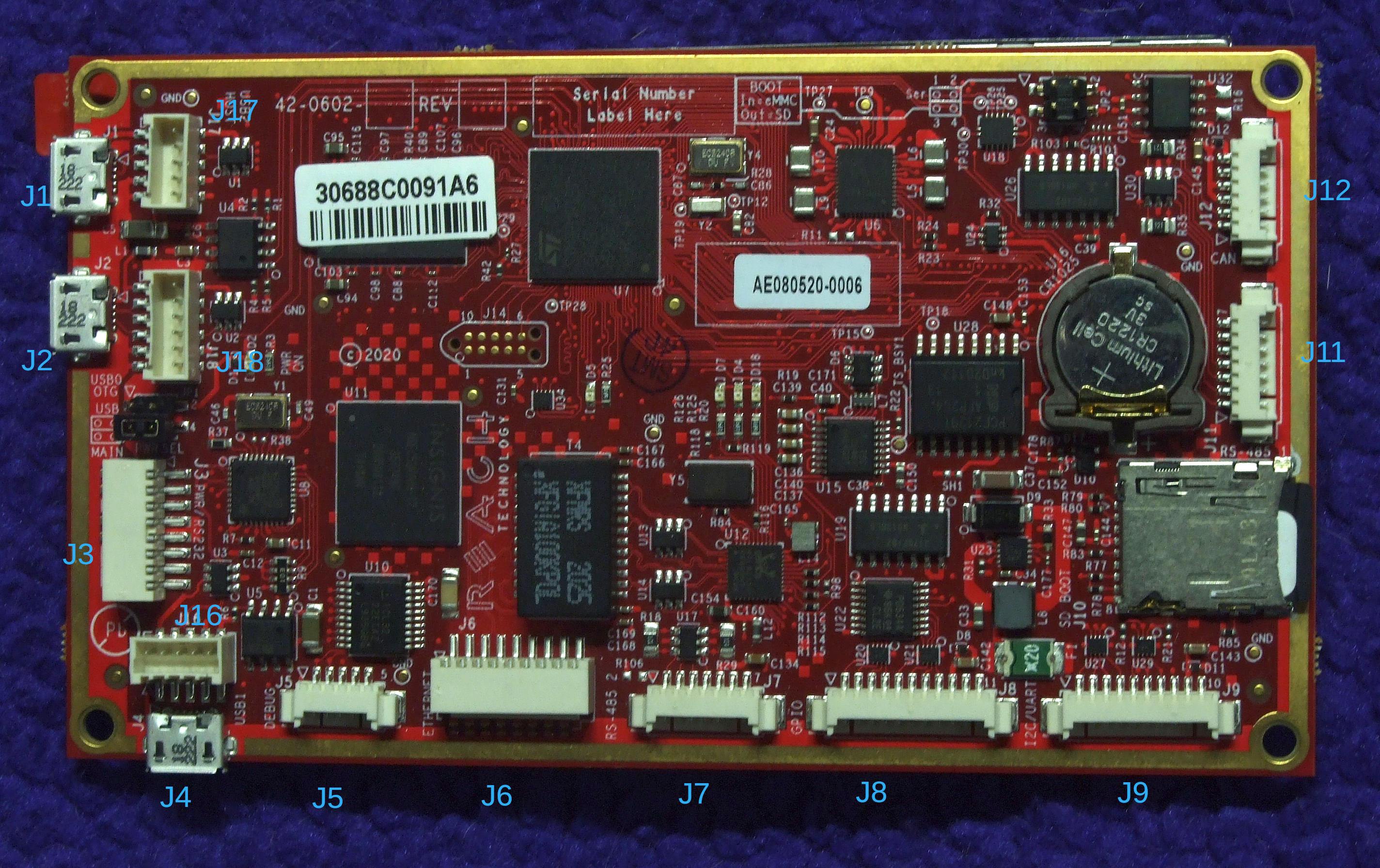
G3MSG I/O Connector Locations
Power
Connect DC power for the G3MSG controller and the touch panel via J31. Although the exact power consumption depends on peripherals as well as the particular touch panel, generally, the package will consume approximately 7W to 15W when the backlight is active.
G3MSG controllers must be driven with a 5V, 3A DC power source.
Footnotes:
- 1
Use Reach Technology “Y” cable, PN 23-0160-18 for 5 VDC.
Console (Debug) Port
Access the controller debug interface via J52. This RS-232 level serial port runs at 115.2k Baud, 8-bit, no parity, 1 stop bit. This port should always be connected during product development. You will need a terminal emulator program or shell that understands ANSI color escape sequences. Examples include Tera Term or PuTTY3 (Windows) or picocom in a bash shell (Linux).
Footnotes:
RS-232 Port
A standard RS-2324 port5 is also available on J36.
Footnotes:
GigaBit Ethernet
A standard 1000baseT network port is available on J67.
Footnotes:
- 7
Use Reach Technology ethernet cable, PN 23-0148-12, if you do not wish to build custom cables.
USB 2.0 Host Port
Connect standard USB 1.0 and USB 2.0 peripherals8 to USB host port 1 (J49 or J1610), or USB host port 2 (J19 or J1710).
Footnotes:
USB 2.0 OTG Port
Note
Currently, the OTG port is only supported in host mode. Contact Reach Technology if you need to use it in device mode.
If the USB 2.0 Host Ports are already in use,11 or you want to use the G3MSG as a USB device12 rather than as a host, you can use the USB 2.0 OTG port on J2 or J18. This port is capable of being either a host port13 or a device port14; J2 is used with a standard micro USB cable.
Footnotes:
- 11
For example by an HID touch controller.
- 12
For example as a Linux Network Gadget for peer to peer USB networking.
- 13
Use Reach Technology USB Host cable, PN 23-0167-12, if you do not wish to build custom cables.
- 14
Use Reach Technology USB Device cable, PN 23-0168-12, if you do not wish to build custom cables.
CAN Bus
A CAN bus connection is available on J1215.
Footnotes:
- 15
Use Reach Technology CAN flying leads cable, PN 23-0146-10, for prototyping.
UART
Warning
Refrain from using the logic level UART on J9 at the moment. It is the same UART used on J3, but without the RS-232 transceiver. Unfortunately, there is currently a hardware design error that does not allow the RS-232 receive pin transceiver driver to be disabled. This wil be corrected in the first board spin.
A logic level16 serial port17 is available on J918.
Footnotes:
I2C Bus
The I2C Bus is also available on J919.
Footnotes:
- 19
Use Reach Technology I2C/UART flying leads cable, PN 23-0149-10, for prototyping.
GPIO
GPIO pins are available on J820
Footnotes:
- 20
Use Reach Technology GPIO flying leads cable, PN 23-0144-10, for prototyping.
RS-485 Port
RS-485 peripherals can be connected to J7 and to J1121. The default mode is full duplex.
Footnotes:
- 21
Use Reach Technology RS-485 flying leads cable, PN 23-0145-10, for prototyping.
Connector Pinouts and Part Numbers
The following sections provide the pinout for each connector and part number for the required mating plug22.
Footnotes:
- 22
For the USB micro AB connectors, we provide the part number of the on board socket. Any standard micro USB plug should mate with this connector.
J1
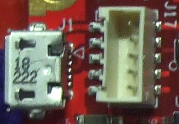
G3MSG USB 2.0 Host Port 2 Connection
5 pin USB micro AB, MOLEX Part # 0475890001
Pin |
Signal |
|---|---|
1 |
+5V |
2 |
Data - |
3 |
Data + |
4 |
NC |
5 |
GND |
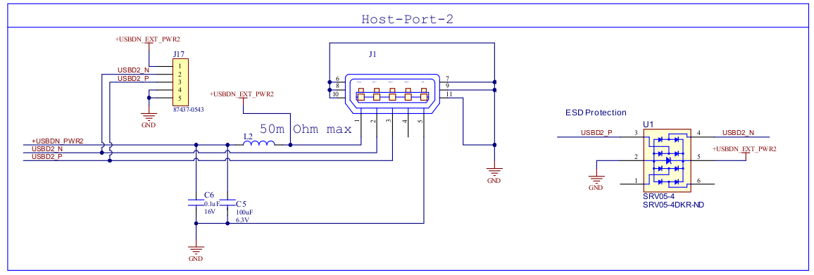
G3MSG USB 2.0 Host Port 2 Schematic
J2
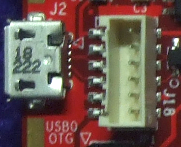
G3MSG USB 2.0 OTG Port Connection
5 pin USB micro AB, MOLEX Part # 0475890001
Pin |
Signal |
|---|---|
1 |
+5V |
2 |
Data - |
3 |
Data + |
4 |
USB_OTG_ID23 |
5 |
GND |
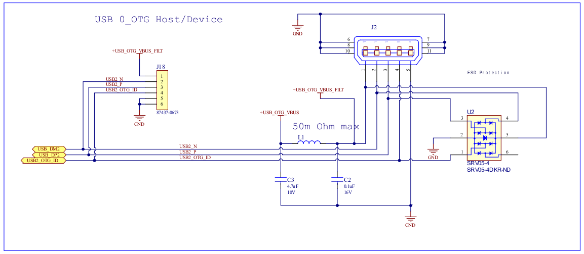
G3MSG USB 2.0 OTG Port Schematic
Footnotes:
- 23
Ground to make J5 a USB Host port.
J3
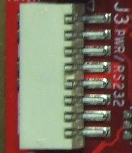
G3MSG Power / RS-232 Connection
8 pin Pico-SPOX, MOLEX Part # 87439-0800
Pin |
Signal |
|---|---|
1 |
|
2 |
|
3 |
GND (power and communications) |
4 |
VIN 5VDC input, powers the board |
5 |
VIN 5VDC input, powers the board |
6 |
GND (power and communications) |
7 |
GND (power and communications) |
8 |
GND (power and communications) |
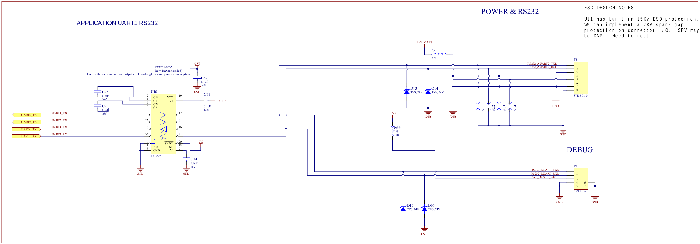
G3MSG Debug Interface, Power, RS-232 Schematic
Footnotes:
J4
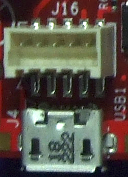
G3MSG USB 2.0 Host Port 1 Connection
5 pin USB micro AB, MOLEX Part # 0475890001
Pin |
Signal |
|---|---|
1 |
+5V |
2 |
Data - |
3 |
Data + |
4 |
NC |
5 |
GND |
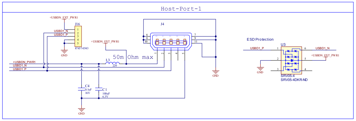
G3MSG USB 2.0 Host Port 1 Schematic
J5
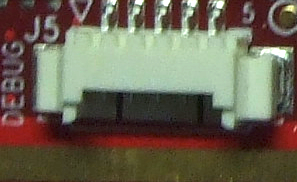
G3MSG Debug Interface Connection
5 pin PicoBlade, MOLEX Part # 51021-0500
Pin |
Signal |
|---|---|
1 |
TxD output ESD protected26 |
2 |
RxD input ESD protected26 |
3 |
CTS |
4 |
GND |
5 |
GND |

G3MSG Debug Interface, Power, RS-232 Schematic
Footnotes:
J6
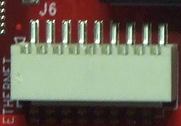
G3MSG GigaBit Ethernet Connection
9 pin Pico-SPOX, MOLEX Part # 87439-0900
Pin |
Signal |
|---|---|
1 |
Bi-Directional pair D1+ |
2 |
Bi-Directional pair D1- |
3 |
Bi-Directional pair D2+ |
4 |
Bi-Directional pair D2- |
5 |
Bi-Directional pair D3+ |
6 |
Bi-Directional pair D3- |
7 |
Bi-Directional pair D4+ |
8 |
Bi-Directional pair D4- |
9 |
Ethernet Shield/GND |
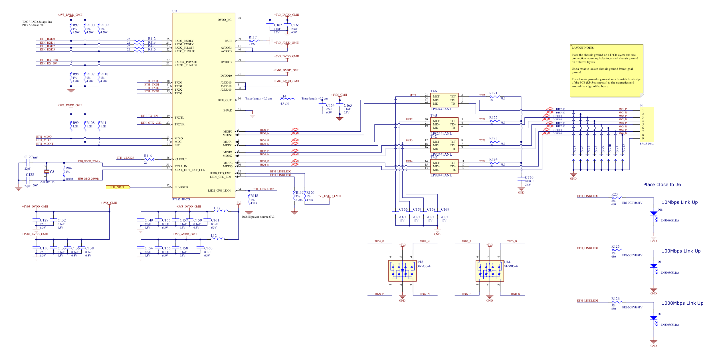
G3MSG GigaBit Ethernet Schematic
J7
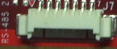
G3MSG RS-485 Port 2 Connection
7 pin PicoBlade, MOLEX Part # 51021-0700
Pin |
Signal |
|---|---|
1 |
Rx H |
2 |
Rx L |
3 |
Tx L |
4 |
Tx H |
5 |
+5V |
6 |
GND |
7 |
GND |

G3MSG RS-485 Port 2 Schematic
J8

G3MSG GPIO Connection
11 pin PicoBlade, MOLEX Part # 51021-1100
Pin |
Signal |
|---|---|
1 |
GP3 |
2 |
GP2 |
3 |
GP1 |
4 |
GP0 |
5 |
GP4 |
6 |
GP5 |
7 |
GP6 |
8 |
GP7 |
9 |
+5V |
10 |
GND |
11 |
GND |
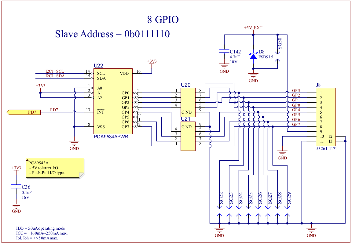
G3MSG GPIO Schematic
J9
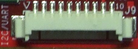
G3MSG UART / I2C Bus Connection
10 pin PicoBlade, MOLEX Part # 51021-1000
Pin |
Signal |
|---|---|
1 |
|
2 |
|
3 |
|
4 |
|
5 |
PF229 |
6 |
I2C2_SCL_BUF |
7 |
I2C2_SDA_BUF |
8 |
GND |
9 |
+5V |
10 |
GND |
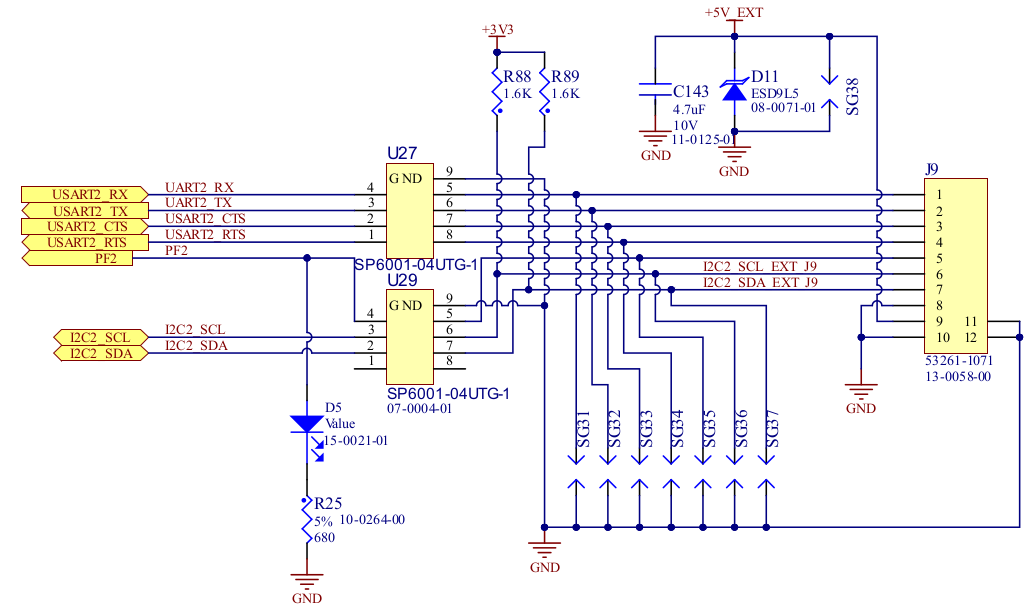
G3MSG UART / I2C Bus Schematic
Footnotes:
J11
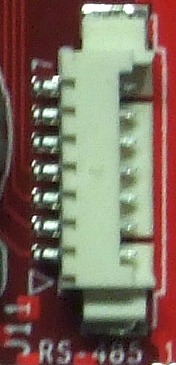
G3MSG RS-485 Port 1 Connection
7 pin PicoBlade, MOLEX Part # 51021-0700
Pin |
Signal |
|---|---|
1 |
Rx H |
2 |
Rx L |
3 |
Tx L |
4 |
Tx H |
5 |
+5V |
6 |
GND |
7 |
GND |

G3MSG RS-485 Port 1 Schematic
J12
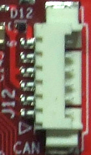
G3MSG CAN Bus Connection
6 pin PicoBlade, MOLEX Part # 51021-0600
Pin |
Signal |
|---|---|
1 |
CAN + |
2 |
CAN - |
3 |
+5V |
4 |
+5V |
5 |
GND |
6 |
GND |
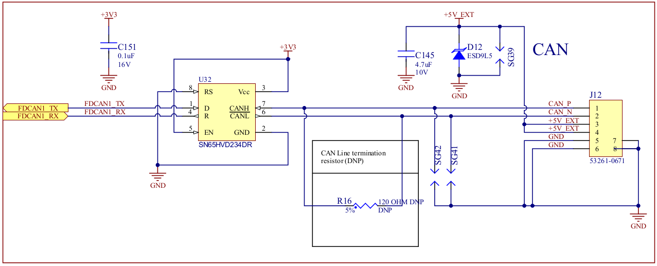
G3MSG CAN Schematic
J16

G3MSG USB 2.0 Host Port 1 Connection
5 pin Pico-SPOX, MOLEX Part # 87439-0500
Pin |
Signal |
|---|---|
1 |
+5V |
2 |
Data - |
3 |
Data + |
4 |
GND |
5 |
GND shield |

G3MSG USB 2.0 Host Port 1 Schematic
J17

G3MSG USB 2.0 Host Port 2 Connection
5 pin Pico-SPOX, MOLEX Part # 87439-0500
Pin |
Signal |
|---|---|
1 |
+5V |
2 |
Data - |
3 |
Data + |
4 |
GND |
5 |
GND shield |

G3MSG USB 2.0 Host Port 2 Schematic
J18

G3MSG USB 2.0 OTG Port Connection
6 pin Pico-SPOX, MOLEX Part # 87439-0600
Pin |
Signal |
|---|---|
1 |
+5V |
2 |
Data - |
3 |
Data + |
4 |
USB_OTG_ID30 |
5 |
GND |
6 |
GND shield |

G3MSG USB 2.0 OTG Port Schematic
Footnotes:
- 30
Ground to make J18 a USB Host port.